Nmos inverter stick and mask layout diagrams, how to draw stick Mosfet physics Solved: design a stick diagram, mask layout (monochrome), and color
[Solved] Question for stick diagram and NMOS and PMOS transistor.. 1
[diagram] hcl stick diagram Nmos inverter stick diagram Stick diagram of two input cmos nand gate || compact stick diagram
Nmos inverter in vlsi
Download nmos and stick diagramStick diagram nmos gate vlsi cmos Stick diagram of cmos inverter circuitMos layers, stick diagram and nmos & cmos encoders used in stick.
[diagram] hcl stick diagramDesign rules for nmos and cmos Cmos inverter designHow to draw stick diagrams ?( vlsi )| simplified| with examples.
Lect5_stick_diagram_layout_rules
Nmos design style examplesStick diagrams for nmos inverter based mosfet combination |vlsi design [solved] question for stick diagram and nmos and pmos transistor.. 1Full tutorial stick diagram|stick diagram in vlsi.
Stick diagram nmos design styleDiagram stick nand gate cmos vlsi input circuit daigram put together been has jce Layout of cmos circuits nmos transistor symbolic layout (stick diagram )Nmos pmos transistor.

Layout diagram of cmos inverter
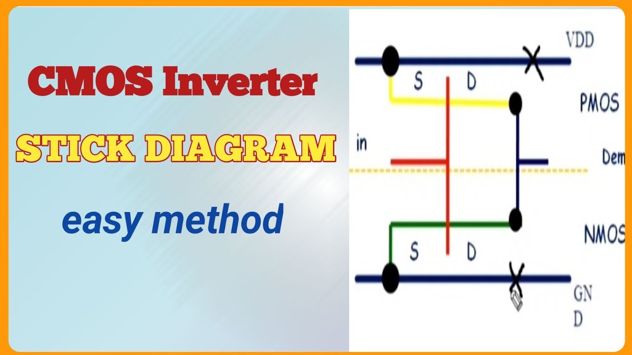
The symbol of (a) a pmos transistor and (b) an nmos transistorCmos 2-input nand and nor gates Nand stick diagram[diagram] stick diagram cmos inverter.
[solved] question for stick diagram and nmos and pmos transistor.. 1Nor nmos stick diagram Stick diagram nmos inverter (hindi)Layout cmos nmos transistor diagram stick symbolic circuits circuit analog integrated studylib.
![[Solved] Question for stick diagram and NMOS and PMOS transistor.. 1](https://i2.wp.com/www.coursehero.com/qa/attachment/22152982/)
Cmos nand gate circuit diagram
Stick diagram of cmos ex-or gate ||explore the wayNmos transistor layout mos section cross ppt powerpoint presentation substrate electrical body source Solved design a stick diagram, mask layout (monochrome) andDownload nmos nor stick diagram.
.


Download NMOS AND Stick Diagram - Educative Site

lect5_Stick_diagram_layout_rules

NMOS DESIGN STYLE EXAMPLES - YouTube

Stick diagram of CMOS EX-OR gate ||Explore the way - YouTube
![[DIAGRAM] Hcl Stick Diagram - MYDIAGRAM.ONLINE](https://i2.wp.com/image.slidesharecdn.com/stickdiagram-vlsidesignunitii-170219114315/95/stick-diagram-9-638.jpg?cb=1487504830)
[DIAGRAM] Hcl Stick Diagram - MYDIAGRAM.ONLINE

CMOS 2-input NAND and NOR gates | Layout diagram | VLSI | Lec-34 - YouTube
![[DIAGRAM] Stick Diagram Cmos Inverter - MYDIAGRAM.ONLINE](https://i2.wp.com/image.slidesharecdn.com/lect5stickdiagramlayoutrules-1226994677707873-9/95/lect5stickdiagramlayoutrules-14-728.jpg?cb=1226965743)
[DIAGRAM] Stick Diagram Cmos Inverter - MYDIAGRAM.ONLINE

Download NMOS NOR stick diagram - Educative Site
